- US - English
- China - 简体中文
- India - English
- Japan - 日本語
- Malaysia - English
- Singapore - English
- Taiwan – 繁體中文
1966 was a long time ago. The Beatles released Revolver. The No. 1 film was The Good, the Bad, and The Ugly. And computers, such as they were, involved paper tape and punch card readers.
That same year, Robert Dennard invented dynamic random access memory (DRAM). Two years later — 55 years ago —on June 4, 1968, the DRAM patent was granted. The rest is history.
To develop the technology, Dennard led a research team at IBM that experimented with binary data on a capacitor as a positive or negative charge. Since capacitors leaked charge, Dennard invented a platform where everything was handled by a single transistor, drastically decreasing the size.
Random access memory (RAM), which employed temporary memory, was widely used at the time, but was complex, bulky and used a ton of power. Large magnetic storage systems required room-sized equipment, while storing only one megabyte of information. Dennard’s idea was to shrink the next generation of magnetic memory to a 25-centimeter square. The trick was condensing RAM into a single transistor. All of a sudden, a computer could hold a billion RAM cells on one chip.
The first RAM chip, the 1103, was released in 1970. In two years, it bypassed magnetic core memory and became the best-selling semiconductor memory chip in the world. By the mid-1970s, it was the standard.
In a recent IBM tribute to Dennard, they describe the shock waves from the discovery: “Over the next five-and-a-half decades DRAM would, generation by generation, evolve...Not only did DRAM memory sweep away the earlier magnetic technologies, it became the foundational technology for an industry that has reshaped human society — from the way we work, to the way we entertain ourselves and even to the way we fight wars.”
Today, DRAM components and modules in various technologies (like DDR, LPDDR, GDDR, HBM) and form factors (components, UDIMMs, SODIMM, RDIMM etc.) are pervasive from smartphones to cloud servers, powering the global economy.
While we’re all familiar with Moore’s Law, Dennard Scaling takes that concept into a deeper technical meaning — the idea that with each generation, you could scale the transistor area down by half, while increasing operating frequency (clock speed) by 40%. In addition, transistors would become cheaper and more numerous in a given space yet keep power consumption constant (for twice the number of transistors).
Dennard even saw the eventual end of Moore’s Law — and Dennard Scaling. An IBM colleague, Russ Lange, remembers it clearly: “Bob and I would always have lively discussions about whether there was going to be an end to the scaling. And he would say, ‘Yes, there’s an end to scaling. But there’s no end to creativity.’”
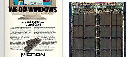
By 1981, Micron exploded onto the DRAM landscape, shipping the first 64K DRAM product. This was the birth of our powerful leadership role in DRAM and NAND. Three years later we released the world’s smallest 256K DRAM product, and in 1987 came 1 megabit DRAM.

Micron 64K DRAM product

Micron ‘We Do Windows’ advertisement and Micron 1Mb DRAM product
Gurtej Sandhu, multi-field inventor, IEEE Andrew S. Grove Award Winner and Sr. Fellow, Technology Pathfinding at Micron, recalls the early innovative days of DRAM, “When I visited the IBM Watson center about 15 years ago, my host took me to Dennard’s office. The office was kept open for visitors and in full working order and I was told that Dennard, who had retired a few years ago, still came there a few hours a week. It was ironic that at the time he invented DRAM, there was more attention given to it by Intel which was looking for a lower cost replacement for SRAM. Lowering the cost of bits was critical to grow the capabilities of computer systems and Intel went to great lengths to design their processor chip to manage DRAM refresh and customize a system level architecture which established DRAM as an integral part of the modern computing revolution.”

Gurtej Sandhu
EEE Andrew S. Grove Award Winner
Sr. Fellow, Technology Pathfinding at Micron
Sandhu adds, “It is a lesson in history we should not forget as we embark on finding memory technology solutions of the future. A successful memory technology implementation will always require a system level approach to design computer architecture and software around it to extract the most benefits for the end customer.”
True to Dennard Scaling, DRAM kept getting smaller and faster. By 2002, Micron was demonstrating the world’s first 1 gigabit DDR (Double Data Rate) DRAM product. Over the years, we continued to lead the charge in DRAM innovation, from early PC DRAM, to graphics, to the current explosion of memory specific to automotive, IoT (Internet of Things) and AI (Artificial Intelligence) devices.
Fast forward to 2021, when Micron released our 1α (1-alpha) node-based DRAM products, with the world’s most advanced DRAM process technology delivering major improvements in density, power consumption and performance.
Notes Scott DeBoer, Micron EVP of technology and products: “With a 40% improvement in memory density over our previous 1z DRAM node, this advancement creates a solid foundation for future product and memory innovation.”
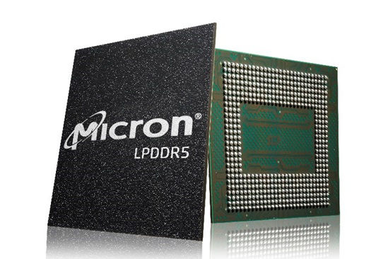
For example, the node enables us to deliver ultra power efficient, reliable memory and faster low-power DDR5 (LPDDR5) operating speeds for platforms that require best-in-class LPDRAM (low power DRAM) performance. The company’s LPDDR5 based on the 1 alpha node, boasts a 15% improvement in power savings, allowing 5G mobile users to perform more tasks on their smartphones without sacrificing battery life.

Micron LPDDR5
Other applications include the industry’s first automotive LPDDR5 DRAM that meets the most stringent Automotive Safety Integrity Level (ASIL), ASIL D. The solution is part of Micron’s new portfolio of memory and storage products targeted for automotive functional safety based on the International Organization for Standardization (ISO) 26262 standard.
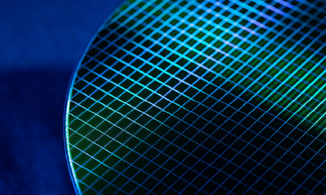
Today, Micron continues to be at the forefront of DRAM advancement, with the release in 2022 of the 1β (1-beta) production node, which boasts a 16Gb per die capacity and a data rate of 8.5Gbps, delivering a 15 percent better power efficiency and upwards of a 35 percent bit density improvement. In an early application of the node technology, Micron LPDDR5X on the 1 beta node will enable high-resolution 8K video recording and video editing in mobile phones.

Micron 1-beta node wafer
Meanwhile, Micron recently announced that our 1γ (1-gamma) DRAM process technology employs revolutionary extreme ultraviolet (EUV) lithography production. We will be the first semiconductor company to bring EUV technology for production to Japan and will ramp EUV into production on the 1γ (1-gamma) node in Taiwan and Japan in 2025.
Robert Dennard's innovation more than 55 years ago invigorated a burgeoning memory industry, including Micron's unparalleled 64k to 1γ DRAM leadership and advancements.
